FIB-SEM (Focused Ion Beam SEM) | High Precision Nano-Analysis
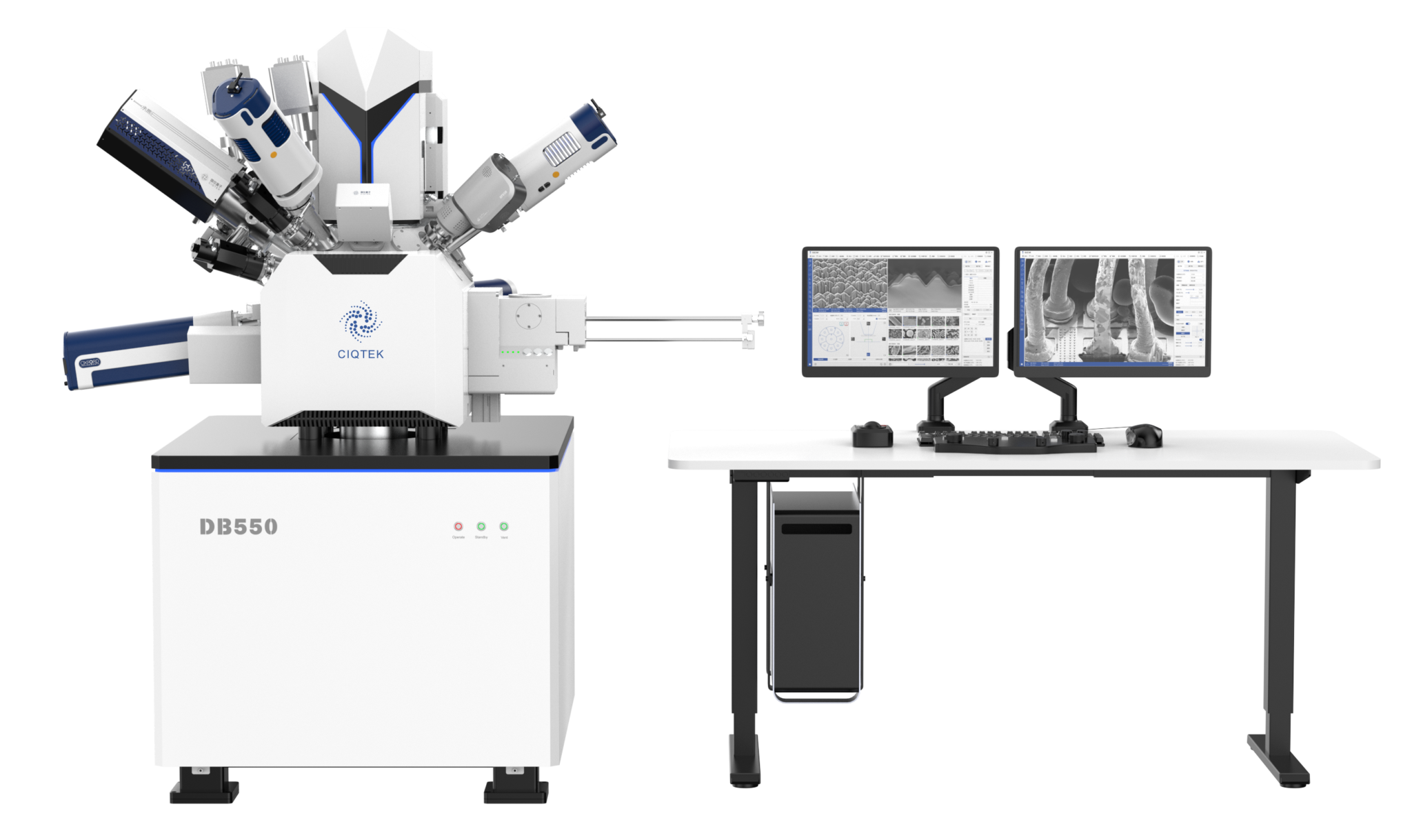
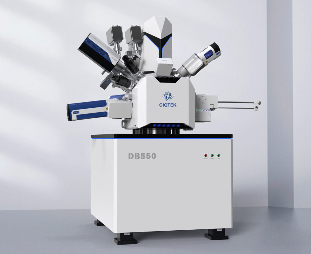
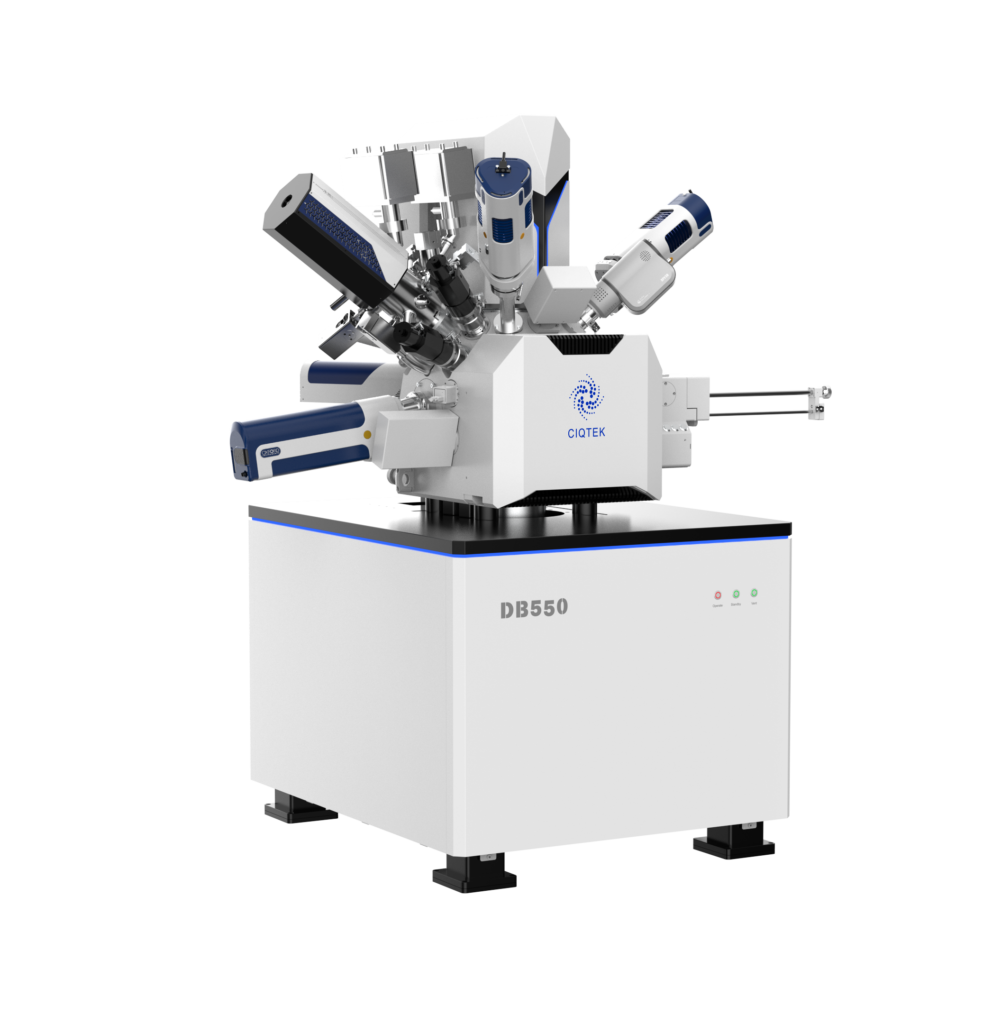
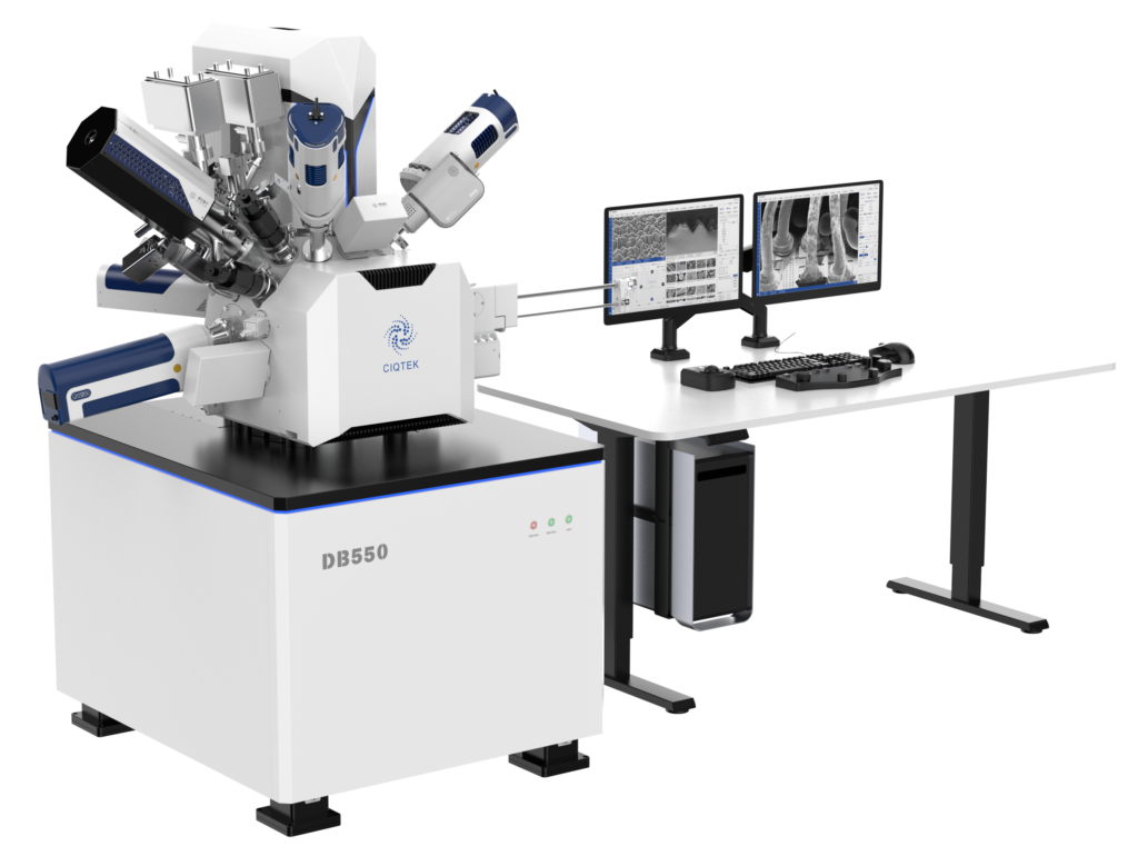
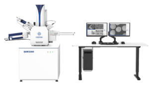
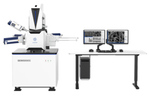
The CIQTEK DB550 is a high-performance Focused Ion Beam SEM (FIB) system that goes beyond traditional electron microscopy by integrating ion beam processing and nano-analysis capabilities
Need a powerful FIB-SEM for your research or manufacturing process? Request a quote today.
The DB550 FIB-SEM delivers unparalleled resolution and precision with its integrated ion and electron beam technology, making it an essential tool for nanotechnology research and industrial applications.
Super Tunnel Electron Optics Technology: Reduces spatial charging effects, enhancing low-voltage imaging performance.
High-Precision Gallium Ion Beam: Features Ga+ liquid metal ion source with nano fabrication precision down to 3 nm resolution.
Integrated Nano-Manipulator: Three-axis system with 10 nm stepper motor accuracy for advanced specimen positioning.
Comprehensive Gas Injection System: Precisely delivers gases for material modification.
Specimen Exchange Loadlock – Supports up to 8-inch samples, reducing contamination and improving sample handling efficiency.
Multi-Mode Advanced Imaging Detectors: Includes Everhart-Thornley Detector (ETD), In-Lens Detector, Back-Scattered Electron Detector (BSED), and STEM Detector for versatile material characterization.
Low-Voltage, High-Resolution Imaging: Optimized for non-conductive and sensitive materials, improving imaging contrast and clarity.
Cross-Industry Application Versatility: Designed for semiconductors, energy research, materials science, and nanotechnology fabrication.
Looking to compare FIB-SEM microscope models? Contact us for pricing and specifications.
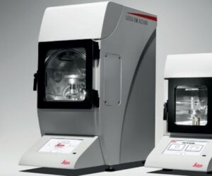
FIB-SEM DB550
DB550 Focused Ion Beam SEM Performance Advantages
FIB-SEM DB550
Unprecedented nano-scale imaging and analysis capabilities
High-resolution imaging across multiple voltage ranges
Precise specimen preparation and manipulation
Reduced spatial charging effects
Improved lens aberration correction
Compatibility with various sample types
All-in-one nano-analysis and fabrication workstation
Advanced semiconductor failure analysis
Cross-section observation capabilities
TEM specimen preparation
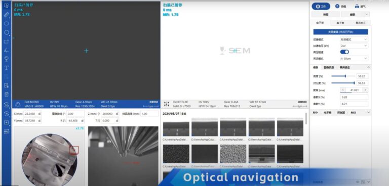
Software Capabilities & Accessories
Integrated user-friendly GUI software
Specimen characterization tools
Cross-section analysis software
Compatibility with multiple signal detection modes
Micro-nano fabrication support
Software Development Kit (SDK) available
Optional image post-processing tools
Detector Options:
Everhart-Thornley Detector (ETD)
In-lens Electron Detector
Retractable Back-Scattered Electron Detector (BSED)
Scanning Transmission Electron Microscopy (STEM) Detector