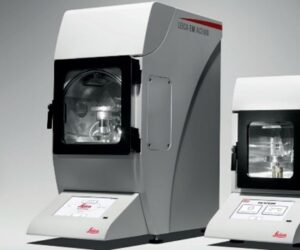
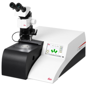
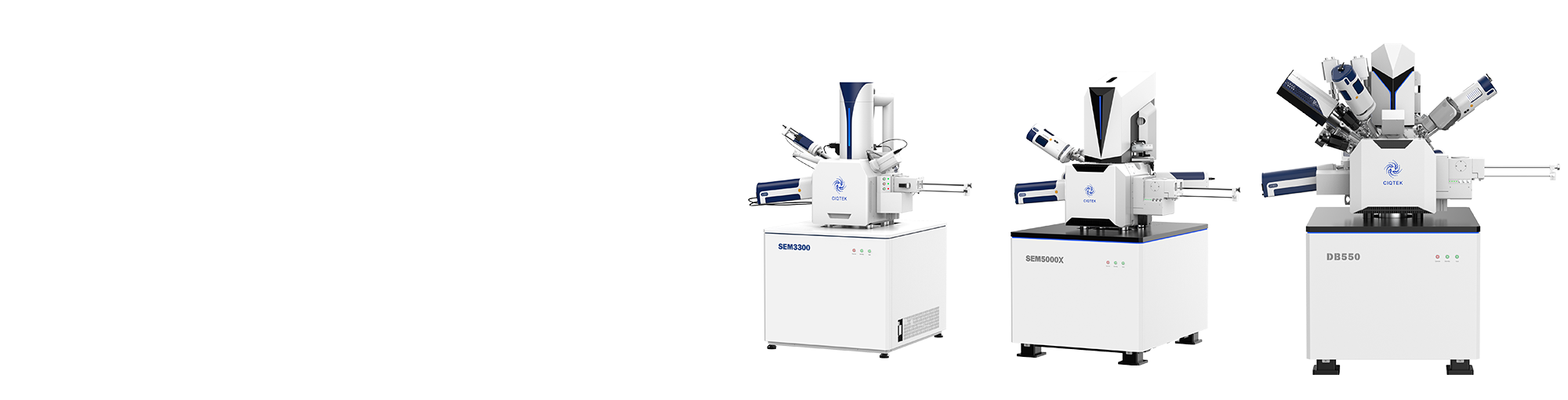
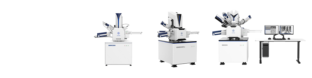
CIQTEK High Resolution SEM Models
A scanning electron microscope (SEM) uses a focused beam of electrons to scan the surface of a sample and produce high-resolution images at the nanoscale. SEM technology is essential across materials science, semiconductor fabrication, quality control, and life sciences — wherever surface structure, composition, or morphology needs to be understood at magnifications far beyond what an optical microscope can achieve. Explore our full-size SEM systems below or contact us to discuss your imaging requirements
Ciqtek

Different Types of Scanning Electron Microscopes

Selecting the right scanning electron microscope depends on your imaging needs, sample type, resolution requirements, and budget. JH Technologies’ high resolution SEM systems are tailored to specific research and industrial applications. 

Whether you’re focused on surface topography, compositional analysis, or microstructural characterization, JH Technologies has a solution engineered to meet your needs.

All systems are backed by expert support and carry the lowest cost of ownership in their class. 

Tungsten Filament SEM–Affordable, Advanced Electron Microscopy

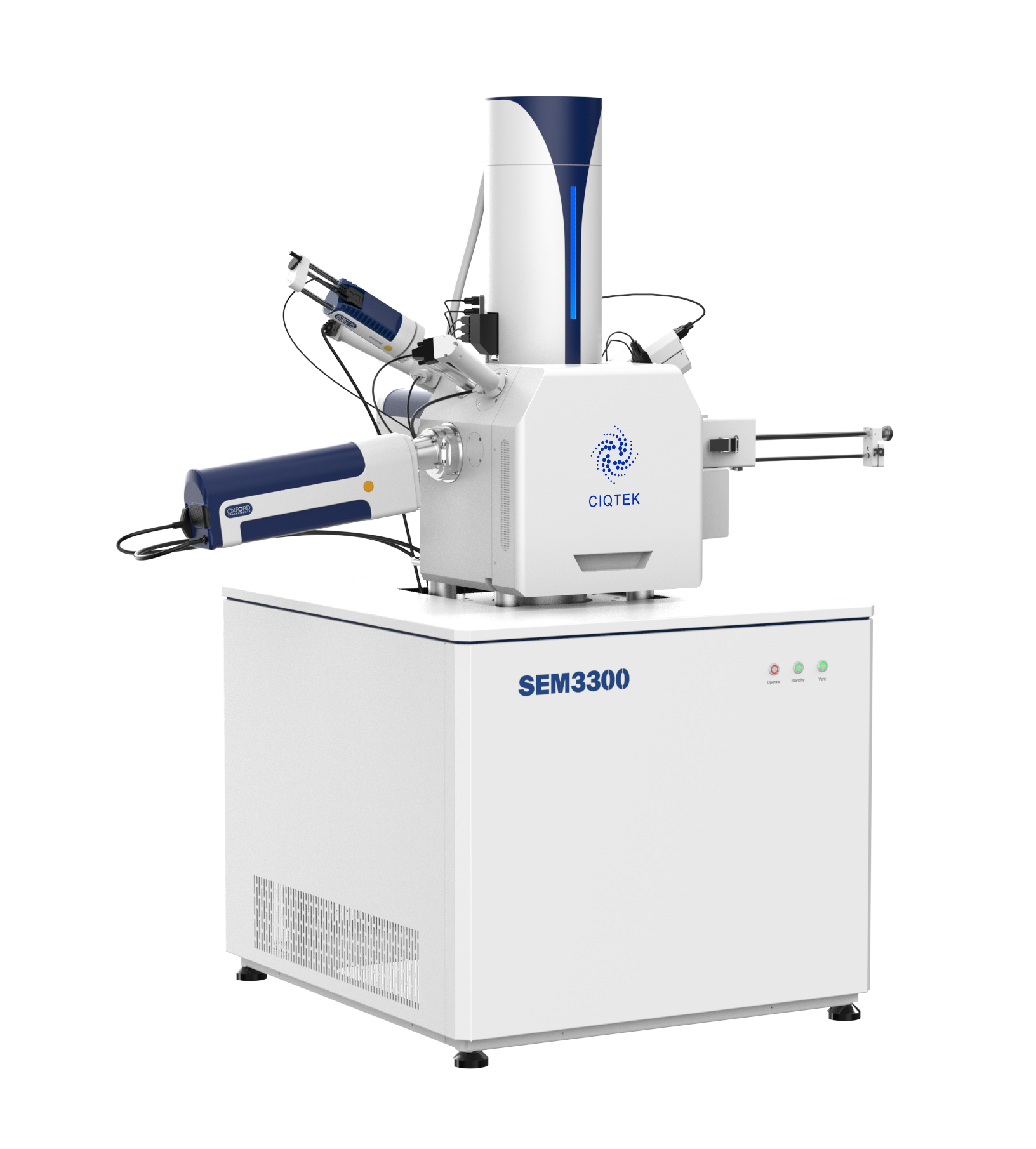
The CIQTEK’s family of Tungsten Filament SEM’s is the ideal choice for labs that need reliable high-resolution imaging and elemental analysis at an accessible price point. Engineered for routine inspection, materials characterization, and quality control, the best scanning electron microscope  family delivers 2.5 nm resolution at 15 kV with automated operation and a flexible expansion platform.

Best suited for: materials science, electronics manufacturing, quality control, and semiconductor research where FE-SEM resolution is not required.

Full-Size Field Emission SEM (FE-SEM)–Ultra-High Resolution Imaging

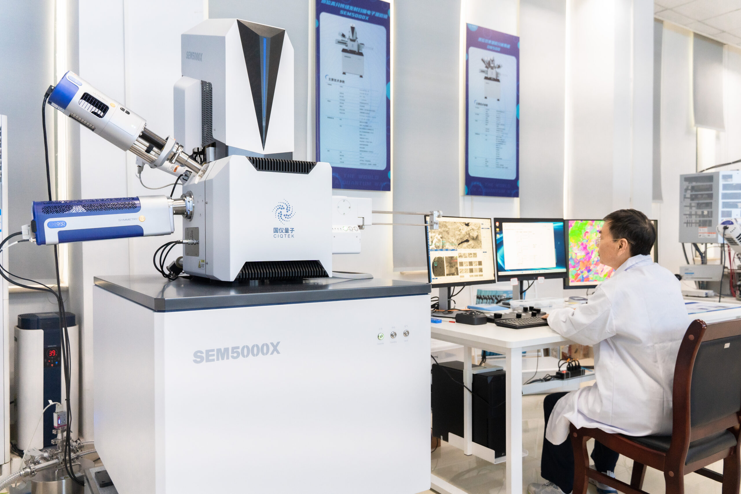
Field emission scanning electron microscopes (FE-SEMs) deliver enhanced resolution and surface detail for high-precision imaging at the nanoscale. The CIQTEK SEM5000X FE-SEM achieves 0.6 nm resolution at 15 kV, making it one of the highest-performing SEM systems available for advanced materials science, semiconductor fabrication, and nanotechnology research.

Best suited for: nano-structural materials research, semiconductor development, and any application requiring sub-nanometer imaging without specimen coating.

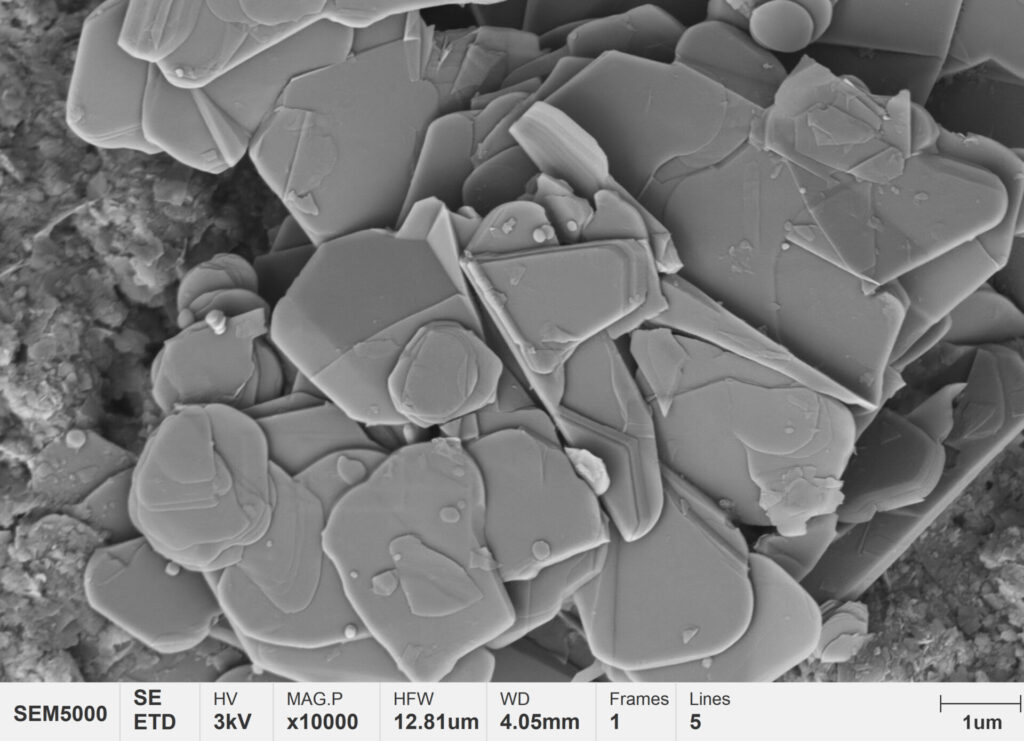
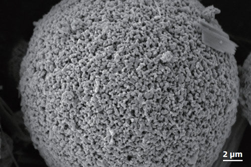
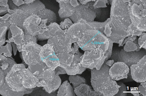
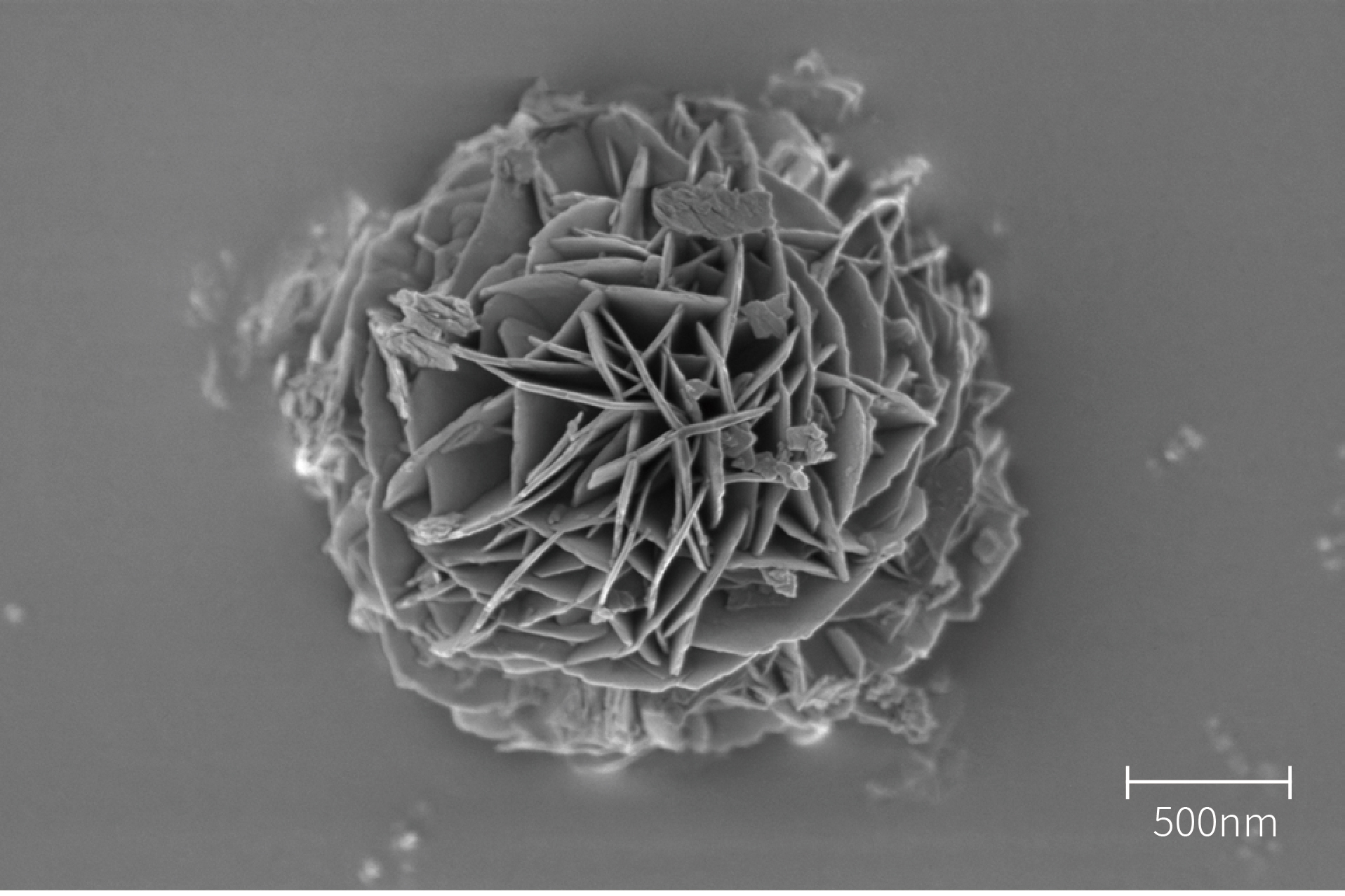
Boron Nitride Nanosheets imaged with CIQTEK Field Emission Scanning Electron Microscope

Focused Ion Beam SEM (FIB-SEM) — Integrated Ion Milling & Nano-Analysis

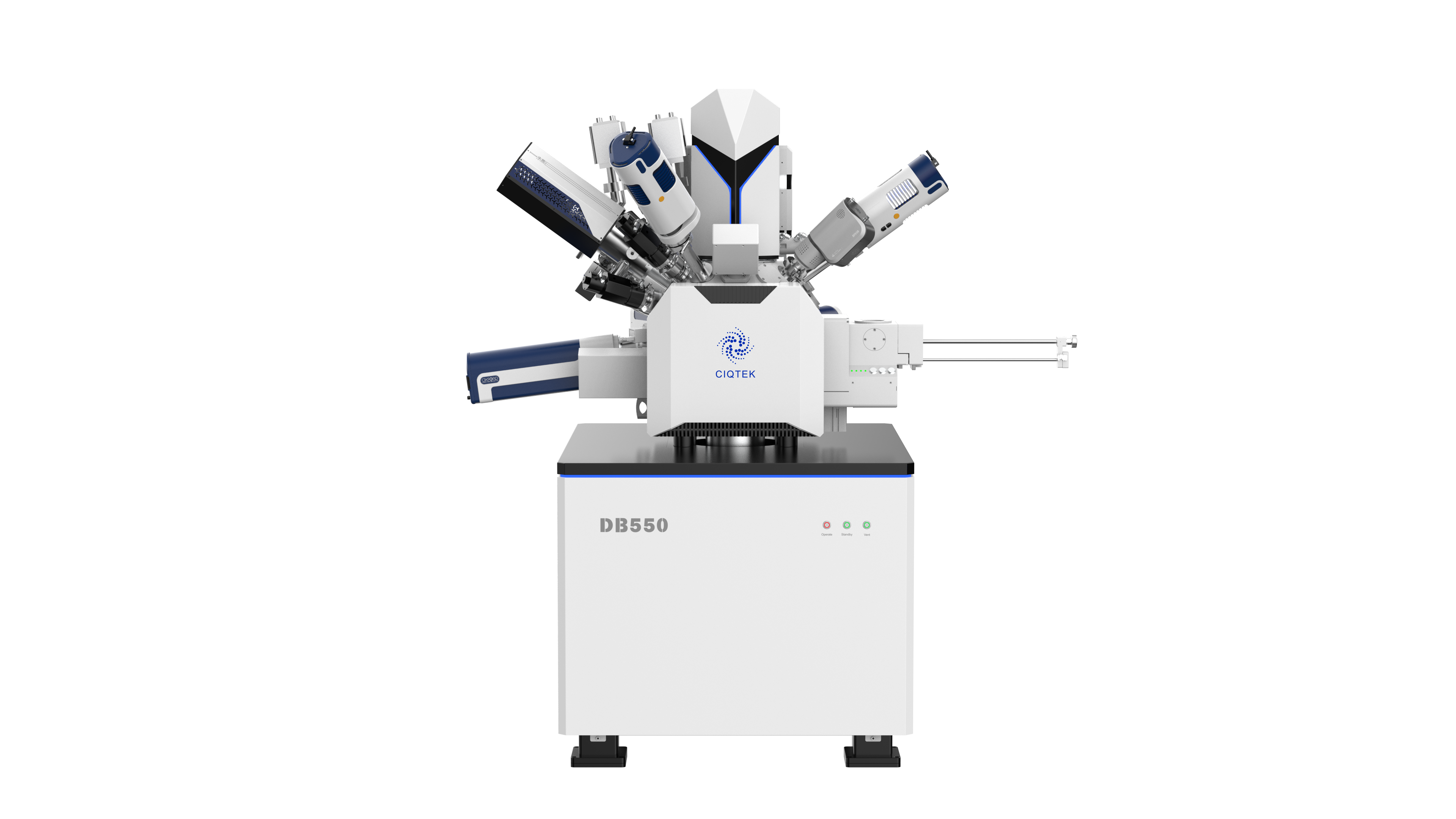
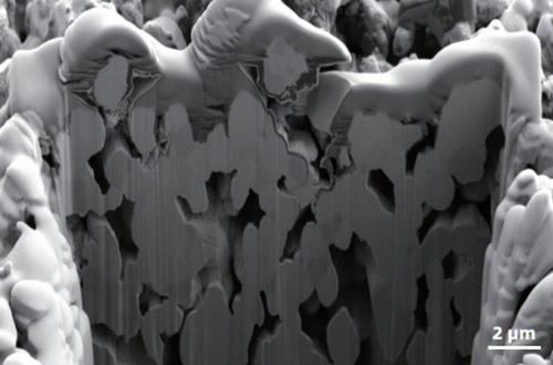
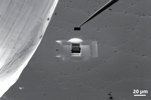
The CIQTEK DB550 FIB-SEM is a dual-beam focused ion beam scanning electron microscope that combines ion beam milling with high-resolution SEM imaging. It is the most capable system in the JH Technologies lineup, designed for semiconductor failure analysis, cross-sectioning, TEM sample preparation, and 3D tomography.

Best suited for: semiconductor failure analysis, nano-fabrication, advanced materials research, and any workflow requiring simultaneous milling and imaging in one instrument.

Explore CIQTEK Scanning Electron Microscope Capabilities

CIQTEK scanning electron microscopes are built to deliver detailed, high-resolution imaging across a wide range of sample types. All SEM models support a comprehensive set of SEM detectors and accessories — including in-lens detectors, backscattered electron detectors, energy dispersive spectrometers (EDS/EDX), and EBSD systems — allowing you to expand your imaging and analysis capabilities as your research evolves. Whether you’re analyzing metals, ceramics, polymers, or battery materials, CIQTEK SEM technology provides the contrast and clarity researchers and engineers rely on.

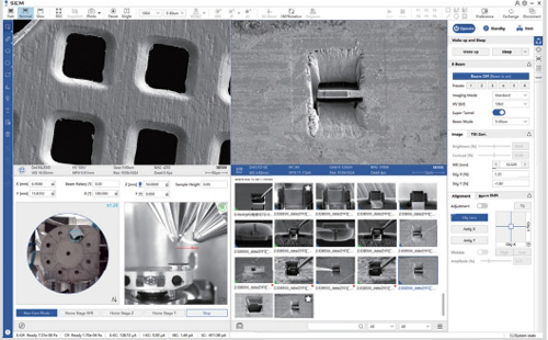
CIQTEK’s scanning electron microscope software is engineered to simplify complex workflows without compromising control. With an intuitive interface and integrated imaging and processing tools, users can navigate all SEM system functions, view live comparative data, and control advanced accessories — all from a single platform. Optional software packages including particle and pore analysis, auto-measure tools, and image post-processing are available across all three SEM models, allowing labs to tailor their sem technology stack to their specific workflow requirements. A Software Development Kit (SDK) is also available for custom microscope control and automation.

CIQTEK SEM systems support a wide range of high-performance scanning electron microscope detectors and hardware accessories, designed to enhance imaging capabilities, streamline workflows, and support advanced analysis across materials science, semiconductors, and nanotechnology.”

Standard SEM detectors included across models:

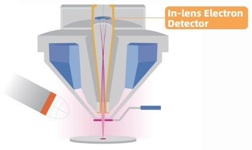
  • In-Lens Secondary Electron Detector — high-contrast surface imaging at low voltages
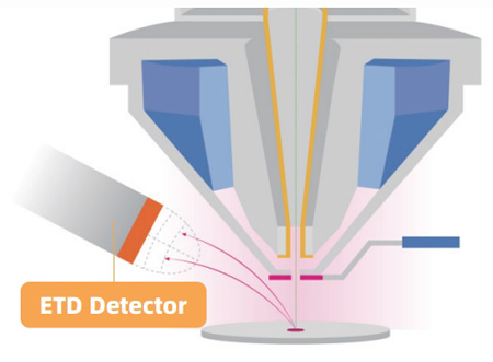
  • Everhart-Thornley Detector (ETD) — standard secondary electron detection for surface topography
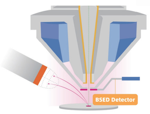
  • Backscattered Electron Detector (BSD) — compositional contrast imaging

Optional SEM detectors and accessories:

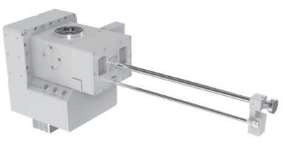
  • Retractable Backscattered Electron Detector (RBSD)
  • Scanning Transmission Electron Microscopy Detector (STEM)
  • Low Vacuum Detector (LVD) — for uncoated or non-conductive samples
  • Energy Dispersive Spectrometer (EDS/EDX) — elemental analysis
  • Electron Backscatter Diffraction (EBSD) — crystallographic orientation mapping
  • Specimen Exchange Loadlock — fast, vacuum-safe sample exchange
  • Nano-Manipulator — in-situ sample handling (FIB-SEM)

These optional components allow users to tailor their SEM setup to specific analysis needs — whether improving surface contrast, capturing internal structures, or increasing throughput in demanding lab environments.

Scanning electron microscopes (SEMs) are essential tools in research, quality control, and product development across a wide range of industries. Their ability to deliver high-resolution surface and cross-sectional imaging at the micro and nanoscale makes them indispensable wherever material structure, composition, or morphology needs to be understood in detail.”

Common SEM applications include:

  • Materials Science — Surface morphology, fracture analysis, grain structure, and phase identification
  • Semiconductors & Microelectronics — Failure analysis, thin-film inspection, circuit edit, and contamination analysis
  • Energy Storage — Battery materials characterization, electrode degradation analysis, and cross-sectional structure
  • Manufacturing & QA/QC — Coating thickness measurement, surface defect detection, and wear analysis
  • Life Sciences — Tissue morphology and cell structure imaging (non-biological SEM preparation required)

“Whether you’re in R&D or production, JH Technologies’ CIQTEK SEM systems provide the imaging depth and analytical capability needed to improve processes, validate performance, and drive innovation. Contact us to discuss which scanning electron microscope model best fits your application

Why Choose JH Technologies for Your Scanning Electron Microscope

Industry professionals across North America — providing advanced electron microscopy solutions and expert guidance at every stage.

As one of the most established scanning electron microscope companies in North America, JH Technologies combines deep technical expertise with a straightforward buying experience. We carry a focused range of high-performance CIQTEK SEM systems, so every model we offer is one we stand behind fully.

  • Lowest cost of ownership in the industry — without compromising resolution or reliability.
  • Expert SEM consultants — help you choose the right scanning electron microscope model for your specific application and budget.
  • Responsive support and service — from experienced microscopy specialists who know the systems inside and out.
  • Fast installation and training — get your SEM up and running quickly, with hands-on onboarding from our team.
  • Trusted by labs across North America — universities, government labs, semiconductor fabs, and industrial manufacturers.

Scanning Electron Microscope Videos

Related Products

Related Blogs

Scanning Electron Microscope — Frequently Asked Questions

What is a scanning electron microscope (SEM)?

A scanning electron microscope is an instrument that uses a focused beam of electrons to scan the surface of a sample and produce high-resolution images. Unlike optical microscopes limited by the wavelength of visible light, SEM technology can resolve surface features down to the nanometer scale, making it essential for materials characterization, semiconductor inspection, and biological imaging.

What are the different types of scanning electron microscopes?

The main SEM types are tungsten filament SEMs, field emission SEMs (FE-SEMs), focused ion beam SEMs (FIB-SEMs), and transmission (TEMs). Tungsten SEMs offer the best value for routine imaging and inspection. FE-SEMs provide superior resolution and are preferred for nanoscale research. FIB-SEMs add a focused ion beam for milling and sample preparation, making them the most versatile option for advanced analysis. TEMs transmit electrons through an ultrathin specimen to reveal internal structures and atomic-scale features, making them essential for nanomaterials, crystallography, biological samples, and high-resolution materials characterization.

What SEM detectors are available?

Modern scanning electron microscopes support a wide range of SEM detectors depending on the signal type and analysis required. Standard detectors include secondary electron (SE) detectors for surface topography and backscattered electron (BSE) detectors for compositional contrast. Optional detectors include energy dispersive spectrometers (EDS/EDX) for elemental analysis, electron backscatter diffraction (EBSD) detectors for crystallographic analysis, and scanning transmission electron microscopy (STEM) detectors. JH Technologies can configure any CIQTEK SEM with the detector suite that fits your workflow.

How do I choose the right scanning electron microscope model?

The right SEM depends on your resolution requirements, sample types, budget, and intended applications. For routine inspection and quality control, a tungsten filament SEM is usually the most cost-effective choice. For sub-nanometer imaging of sensitive or uncoated samples, an FE-SEM is the better fit. For cross-sectioning, TEM sample preparation, or semiconductor failure analysis, a FIB-SEM is the right tool. Contact JH Technologies and we’ll help you identify the best scanning electron microscope for your lab.

Keywords –

what is an sem microscope (110/mo), scanning electron microscope models (1000/mo), scanning electron microscope detectors (50/mo), sem detectors (50/mo), scanning electron microscope companies (140/mo), scanning electron microscope vendors (40/mo), best scanning electron microscope (50/mo), sem technology (40/mo), scanned electron microscope (30/mo)
Contact Us

For additional details and pricing please contact us                                                                                                                                     

Get Your Free Price Quote